Photo Etching PCBs
Another quick howto I've been meaning to write for quite a while. There are several detailed guides available on the net, so I'm not going to go into too much detail except on some parts that took me a while to get ironed out.
Definitions:
PCB - Printed Circuit Board - a laminate generally composed of layers of fiberglass and copper. The ones we start with here are pre-coated with a photosensitive compound that makes this whole process possible.
Developer - The chemical solution you use to dissolve the photosensitive coating from the PCB where it has been exposed to UV light
Exposing - Allowing light to strike the coated PCB where we want to remove copper later in the etching stage. Generally facilitated by a fluorescent bulb positioned in a "light box," although I suppose if you were resourceful and had a light meter, it would be possible to use sunlight for the purpose.
Etchant - A chemical solution that dissolves copper, but not the photosensitive coating that's left on after exposing and developing our PCBs.

*Positive coated PCB - So far, I've tried Injectorall and MG Chemicals brands, seem to have better luck with the MG stuff.
*Light box - We just tossed together a really basic little light box that has a single fluorescent UV bulb in it, probably would get better results for large PCBs by using one with multiple bulbs, but since I tend to play with smallish stuff it's not a big deal. It's probably fine to use a grow-light or other full spectrum bulb, but we just went ahead and started out with a bulb made for the purpose.
*Mask - From what I've heard, the best thing to print your mask onto is thick tracing paper, but since we already had some of those acetate transparency sheets, I've just been using them. Laser printers are definitely the way to go, the toner they use for printing is much more opaque than ink and they generally have much better resolution than inkjet printers. When you print your mask out, you want to end up with black where the copper should be and clear where you don't want to end up with any copper. Very carefully (especially when doing boards for SMT stuff with teeny traces) check your mask for any bubbles, scratches, or whatever and fix them with a black sharpie marker before you get started with exposing and etching the board. To get the easiest to work with solder pads for thru-hole connections, draw a little square for the pad (easier to solder than a circle for whatever reason - seems to flow nicer) then put a clear dot in the center so that when you etch the board, it will leave a little divet for centering the drill. When you expose the board, you want the toner side against the PCB, so mirror the layout for SMT stuff and don't for thru-hole if you draw your layout from the perspective of looking down at the top of the finished board. Of course, use your brain and mirror when appropriate if you're mixing SMT and thru-hole (as I generally do lately,) or making double sided boards. If you use the transparency film, sometimes it has a matte coating applied to one side for inkjet printers - this coating is a pain in the butt to deal with in a wet environment (like the bathroom you end up spinning boards in,) so wash it off with some steel wool in a sink before you get started.
*Developer - Don't even bother with the straight sodium hydroxide solution recipes you'll find a lot of on the net - it's very very temperature and concentration sensitive, and it's very easy to over-develop the board where the traces will all lift off leaving you with a bare PCB. Instead, use a recipe similar to the following that uses both sodium hydroxide and sodium silicate to make a much friendlier developer. Or, of course you could track down a commercial version of the same thing if you're feeling a little less like a recreational chemist:
Making silicate based developer:
Ingredients:
*Water, 480mL - Tap water if you don't have too many minerals or a lot of chlorine in yours, probably not a bad idea to use distilled (as in grocery store distilled, nothing fancy) water if yours isn't too pure by itself. Had no problems so far using well water.
*Sodium Hydroxide, 14.5g - Aka lye aka caustic soda. Easy to get in the form of Red Devil drain opener (double check before you use it, but what I've seen is anhydrous (or at least as anhydrous as lye gets in reality) lye granules. Tricky to measure out accurately as it sucks water out of the air really quickly, so work fast and don't get it on your fingers!
*Sodium Silicate solution, 40% ~10mL - Aka "Water Glass." Harder to find than sodium hydroxide, but still not too hard to track down. Gets used for glazing ceramics and according to the wikipedia article I just linked to, a bunch of other things as well. We just happened to have some lying around, so I can't name a particular source for it. The trick here is that I'm not completely sure what the concentration of the solution I've been using is. It was originally 20%, but the stuff will gradually precipitate out of solution and this was definitely an old jar of solution. If you have problems with your board overdeveloping (traces showing clearly, then lifting off,) maybe try adding a bit more silicate solution.
So, to mix the stuff up, start with say 30mL water, slowly stir in your sodium hydroxide (this part is definitely an exothermic reaction, so take it slow to keep from boiling the water and causing problems,) add the sodium silicate, then the rest of the water. Voila!
*Water - Used as a stop-bath when you develop the boards, and for wiping up any developer or etchant that gets dribbled on the bathroom counter before it stains/dissolves things.
*Etchant - Your usual ferric chloride etchant that's still available from most any halfway decent electronics supplier. Fresher stuff works better, or you can actually electroplate out the copper from old etchant to re-use it, but I'll leave that as an exercise for the reader :).
*Tubs for developer, water, and etchant - I use some little rubbermaid bins for this purpose, some people use fancier arrangements for the etchant that heat the etchant and blow bubbles to make things go faster. Swishing the whole deal around by hand works fine for me.
*Thin bit of plate glass - Make sure it's not the kind with a UV blocking coating :)
*Split hose thingies - Used for double sided boards, described later
*Tweezers
*Timepiece
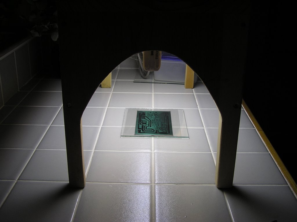
Draw up and print your mask. Double check that it's in good shape, that the scale is right, and that it's pretty. In some sort of place without direct sunlight and a nearby water source (the bathroom,) peel off the protective cover from your PCB, place it facing up on the surface, put your mask toner side down on the board, place the glass over this to press the mask down against the PCB. Put your light source over the whole arrangement, turn on the light for a bit (4.5 minutes with my setup, you'll have to play with yours to see what works.) Turn off the light, gently remove the glass and mask. Drop the PCB into the developer solution and gently agitate while closely watching the board. The areas that were exposed to light should fairly quickly dissolve and dissipate, leaving only the areas that were kept in shadow by your mask. As soon as it looks done, pluck the board out with tweezers (being careful not to scratch the resist that's left behind) and put the board in the water bath, and agitate to rinse off any excess developer. Ideally, at this point, you just need to drop the board into some etchant and etch as usual. Realistically, you'll have to tweak exposure times and such before you get your system dialed in, but it's not that big of a deal.
You want to get the exposure time (the single biggest variable when you're using a good silicate developer solution) where it's adequate to completely remove all the resist where light hits it, but not much longer to prevent the shadowed areas from being exposed to too much UV. Injectorall (I think) makes a nice little mask that's basically a pair of triangles with their tips touching (ASCII art version- |><| ) that you can use to gauge exposure time. If the area with the tips touching has too much copper left when it's all done, your esposure time is too short, if the tips aren't touching at all when it's done, the time was too long, if it's perfect than so is your exposure time!
I haven't done much with double sided boards since what I generally do is single-run stuff and I don't mind using jumpers, but from my limited experience it's not too hard to print alignment marks on the top and bottom masks that line up with the real life corners of the PCB, then expose the two sides individually before dropping the board into developer and then etchant. When developing or etching double sided boards, make 4 split hose thingies and use them to make sure that developer and etchant can circulate around both sides of the board. Split hose thingies are short (say 1/2 inch) bits of small (3/16 inch ID) vinyl (or similar) hose with a cut running down the axis such that they can be stuck on the edges of your board to make the board itself stand off the bottom of the developer/etchant tub. It's important to remember not to run traces too close to the edge of the board if you're going to use this technique - I generally try to leave about a quarter inch margin around layouts for this reason and because cutting the coated boards (they're all cut at some point) generally leaves a bit of funky coating on the edges that wouldn't be good to use for electrical paths.
Sources/Resources:
Digikey - Coated PCBs, parts to put on the finished boards.
Radio Shack - As much as I hate recommending this company, they're who I generally get etchant from.
Your local grocery store - lye for making developer solution.
http://www.electricstuff.co.uk/pcbs.html - A better, more thorough howto. Also where the inspiration for the above developer recipe came from.
Anyhow, that's all I've got to say about photo-etching PCBs for now!
posted by Slartibartfast @ 5:45 PM
![]()

0 Comments:
Post a Comment
<< Home